Overview of 3D Integration

3D Integrated Circuits (3D IC) represent a major advancement in electronics, offering enhanced performance and functionality through vertical stacking. This section covers their evolution, basic principles, and benefits.
Evolution of Integrated Circuits
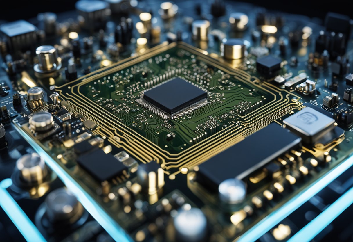
Integrated circuits (ICs) have evolved significantly since their inception. The journey began with planar ICs, where components are placed on a flat surface. Over time, the industry pushed the limits of what could be achieved with a two-dimensional layout.
With the emergence of three-dimensional integrated circuits, components can now be stacked vertically. The challenges of Moore’s Law partly drove this evolution, as traditional scaling methods encountered physical and economic limits.
Basic Principles of 3D IC
3D ICs leverage vertical stacking techniques such as through-silicon vias (TSVs) and Cu-Cu connections. Each layer of the stack contains ultra-thin layers of ICs. These layers are interconnected vertically, allowing them to work as a single unit.
The technology behind 3D integration involves precise alignment and bonding of different layers. This method optimizes performance, power consumption, and area efficiency by bringing components closer together.
Benefits of Three-Dimensional Integration
Three-dimensional integration brings numerous advantages to IC design. One key benefit is improved performance, as shorter interconnects reduce signal delay and power consumption. This makes 3D ICs ideal for high-performance computing applications.
Another advantage is space efficiency. By stacking layers, 3D ICs can pack more functionality into a smaller footprint, making them suitable for compact devices like smartphones and wearables. Challenges remain, such as managing heat dissipation and ensuring reliability, but ongoing research continues to address these issues.
Technologies Enabling 3D ICs

3D Integrated Circuits (ICs) leverage advanced technologies to achieve higher performance, reduced power consumption, and compact designs. Key technologies include Through-Silicon Vias (TSVs), wafer bonding techniques, and interposer technology.
Through-Silicon Vias (TSVs)
Through-silicon vias (TSVs) are vertical electrical connections that pass through silicon wafers or dies. They enable shorter interconnect lengths between different layers of the 3D IC, resulting in faster signal transmission and reduced power consumption. TSVs are critical for densely packed circuits and are used in 3D packaging to connect stacked dies efficiently. By providing a direct path for electrical signals, TSVs reduce the need for long, power-hungry interconnects.
Wafer Bonding Techniques
Wafer bonding techniques are essential for 3D ICs, allowing multiple wafers or dies to be stacked and electrically connected. Several methods include oxide bonding, adhesive bonding, and hybrid bonding.
- Oxide Bonding: Uses an oxide layer to bond wafers.
- Adhesive Bonding: Relies on adhesives to join wafers.
- Hybrid Bonding: Combines oxide and adhesive bonding for stronger, more reliable connections.
These techniques ensure the stacked layers are well-aligned and maintain structural integrity and electrical performance.
Interposer Technology
Interposer technology employs a substrate, usually silicon, to connect multiple dies side by side or in a stacked configuration. It acts as a bridge for electrical signals and power distribution.
- 2.5D Packaging: Uses a silicon interposer to place dies next to each other.
- 3D Packaging: Stacks dies vertically using an interposer with through-silicon vias (TSVs).
This results in improved thermal management and reduced latency, enhancing overall device performance. Interposers are crucial in advanced technology nodes, enabling higher integration and functionality.
3D IC Design and Manufacturing Challenges

3D Integrated Circuits (3D ICs) face unique challenges in their development process, primarily focusing on thermal management, reliability, and manufacturing complexity. These challenges are critical and require specialized solutions to enhance performance and efficiency.
Thermal Management
One of the major challenges of 3D ICs is managing heat. Due to the stacking of multiple layers, heat dissipation becomes difficult. The power density is significantly higher compared to traditional 2D chips. This can lead to hot spots, which might degrade the performance or cause device failure.
Thermal analysis helps identify heat-related issues by simulating different scenarios. Effective cooling solutions like heat sinks or building efficient pathways for heat removal are essential. Proper thermal management ensures the longevity and reliability of 3D ICs and maintains consistent performance levels.
Reliability Concerns
Reliability in 3D ICs extends beyond thermal management. These circuits face signal integrity problems, electrostatic discharge, and mechanical stress. Integrating multiple layers can increase the chances of defects and failures, making reliability testing crucial.
Robust testing methods must be employed to detect early failures. Techniques such as built-in self-test (BIST) and design-for-testability (DFT) are often used. They help identify potential reliability issues that could compromise the entire system’s performance over time.
Manufacturing Process Complexity
The manufacturing process of 3D ICs is more complex than traditional methods. It encompasses several advanced techniques, such as through-silicon vias (TSVs) and micro-bumps, to interconnect various layers. These processes require precise control and advanced equipment.
TSVs are vital for vertical connections, but their implementation is challenging due to alignment and bonding issues. Achieving seamless integration without defects requires meticulous planning and execution.
Applications of 3D Integrated Circuits

3D Integrated Circuits (3D ICs) are transforming various technology sectors by enhancing performance, reducing power consumption, and shrinking device sizes. Key areas benefiting from these advancements include consumer electronics, high-performance computing, and mobile and cloud technology.
Consumer Electronics
3D ICs play a significant role in consumer electronics by enabling more compact and efficient devices. Stacked memory in devices like SSDs and DDR4 RAM enhances storage capacity and speed. High bandwidth memory (HBM) technology, used in graphics cards and gaming consoles, offers rapid data transfer rates.
Smartphones and tablets benefit from improved memory devices and processors, resulting in faster performance and better energy efficiency. This integration supports high-resolution screens and advanced functionalities in smaller form factors. Wearable technology, like smartwatches, also significantly improves battery life and processing power through 3D ICs.
High-Performance Computing
In high-performance computing (HPC), 3D ICs address the demand for greater computational power and energy efficiency. Hybrid memory cube (HMC) technology provides faster memory access speeds, crucial for applications requiring large data processing, such as scientific simulations and data analytics.
By vertically stacking processors and memory, data transfer speeds increase while power consumption decreases. This setup allows for higher performance with lower latency, benefitting supercomputers and data centers. HPC systems utilizing 3D ICs are better equipped to efficiently handle complex computations and large-scale simulations.
Mobile and Cloud Technology
3D IC technology benefits mobile devices and cloud computing platforms significantly. In mobile devices, 3D ICs enable more powerful and energy-efficient processors, enhancing the capabilities of smartphones and tablets.
Cloud computing benefits from improved performance and lowered energy consumption in servers and storage systems. Enhanced memory devices and processors support high-speed data access and transfer, improving the overall efficiency of cloud services. High-bandwidth memory also plays a crucial role in facilitating fast data transactions in cloud infrastructures.
Advancements and Trends in 3D IC Technology
3D IC technology is advancing rapidly, significantly improving performance, power efficiency, and miniaturization. This section discusses key developments, including heterogeneous integration, breaking scaling limits of traditional 2D ICs, and future research directions.
Heterogeneous Integration
Heterogeneous integration combines different types of semiconductor devices and materials in one package. By integrating logic, memory, and other components on multiple silicon wafers, 3D ICs achieve higher performance and lower power consumption. For instance, nano crossbar phase-switching and graphene NEMS electrostatic discharge protection devices are noteworthy advancements in this space Advances in 3D Heterogeneous Structures and Integration for Future ICs.
The use of through-silicon vias (TSVs) is also critical. These allow vertical electrical connections through silicon wafers, further enhancing data transfer rates and reducing energy use. Additionally, integration at the die level supports compact vertical inductors, which enhances power efficiency and performance.
Scaling Beyond Traditional 2D Limits
3D IC technology overcomes the limitations of Moore’s Law by stacking semiconductor devices vertically. This approach significantly reduces interconnect lengths and increases communication density, leading to faster data transfer rates and lower latency Three-Dimensional Integrated Circuit (3D IC) Key Technology: Through Silicon Vias.
With wide I/O memory, data transfer between layers is faster and more efficient, supporting high-performance computing applications. Vertical stacking’s smaller form factor allows for more functional density within the same physical footprint, enabling continued advancements in device miniaturization.
Future Directions in 3D IC Research
Future research in 3D ICs is looking into integrating electronics and photonics for even higher data transfer capabilities. A promising direction is adding a photonics I/O layer to achieve terabit-per-second-scale connectivity, which can significantly enhance overall performance Building 3D integrated circuits with electronics and photonics.
Researchers are also exploring new materials to advance 3D IC technology further. For example, two-dimensional (2D) materials like graphene could offer unique properties, such as increased flexibility and conductivity, supporting future IC innovations 3D integration of 2D electronics.
Additional investigations include developing more reliable and efficient thermal management solutions to handle the increased heat generation in densely packed 3D ICs. Such advances will help maintain high performance while ensuring device longevity and stability.
Frequently Asked Questions
3D integrated circuits (ICs) offer higher performance and efficiency than traditional ICs. They are used in various high-tech applications and have unique design and packaging challenges.
What are the primary applications of 3D integrated circuits?
3D ICs are primarily used in advanced consumer electronics, telecommunications, and high-performance computing. These ICs enhance devices such as smartphones, tablets, data centers, and AI systems by providing faster processing and increased functionality.
How does 3D IC packaging differ from traditional IC packaging?
3D IC packaging involves stacking multiple chips vertically and connecting them through vertical interconnects. In contrast, traditional ICs are laid out on a single layer. This vertical stacking allows for reduced footprint and improved performance.
Can you list the advantages and disadvantages of 3D integrated circuits?
Advantages:
- Higher performance and faster data transfer
- Reduced power consumption
- Smaller footprint
Disadvantages:
- Higher manufacturing cost
- Increased complexity in design and testing
- Thermal management challenges
What are the design challenges associated with 3D integrated circuits?
Designing 3D ICs involves dealing with thermal management, ensuring proper alignment of stacked layers, and managing power distribution. Designers also need to address signal integrity and reduce potential interference between layers.
How does monolithic 3D integration improve upon standard 3D IC integration techniques?
Monolithic 3D integration builds multiple active silicon layers with vertical interconnects on a single chip. This integration method provides even higher density and performance than traditional 3D IC stacking techniques, allowing for more efficient use of space and resources.
In what way do 2D and 3D integrated circuits differ in terms of structure and performance?
2D ICs have all their components laid out on a single plane, leading to larger physical size and slower interconnects. On the other hand, 3D ICs stack multiple layers vertically, leading to smaller size, higher speed, and greater functionality. This vertical structure allows for more compact and efficient designs.


